Hi-Potential Test Fixture

Background Information

The cell interface can be exposed to high voltages. It is necessary to ensure that the safety mechanism in the CI circuit functions properly. A test fixture that uses a Hi-Pot test unit will be used for the examination of the mechanism.

Problem Definition

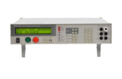
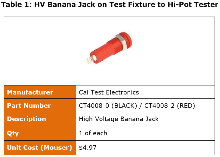
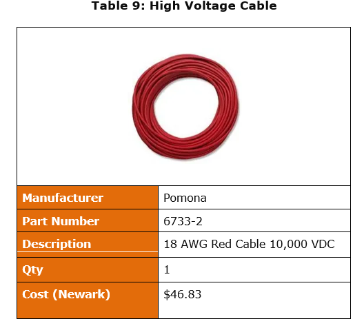
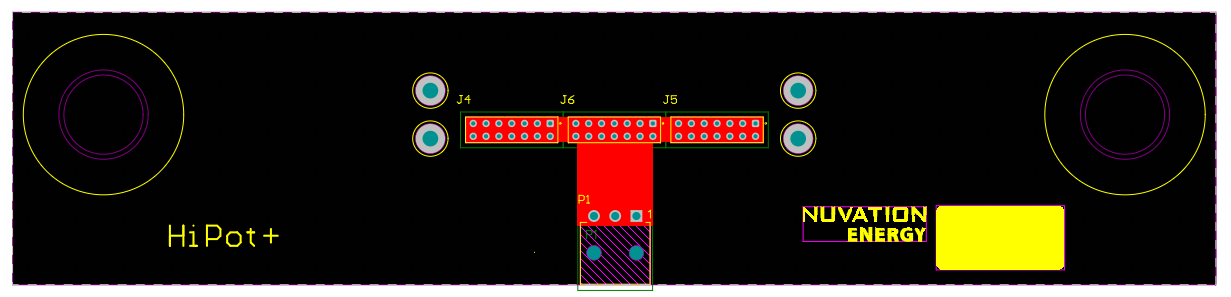
  • Need a safe, repeatable manufacturing test to verify the CI-24 isolation barrier by applying ~7.2 kV AC for 5 s across HV/LV and logging a clear pass/fail.

Goals / Objectives / Constraints

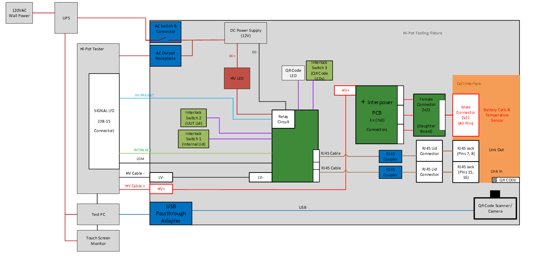
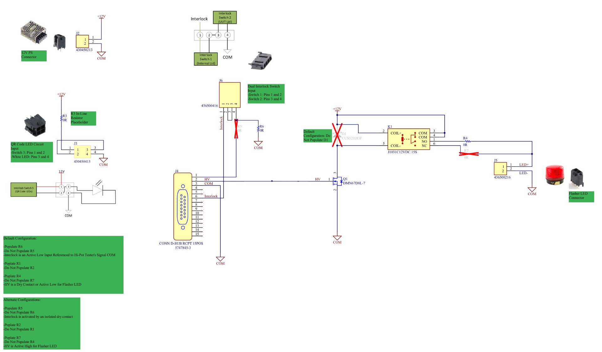
1. Safety first: dual door/lid interlocks tied to the Hi-Pot interlock; a third switch only powers the QR-illumination LED; PC is not in the safety chain.

2. Operator flow: z-axis jib where operator clamps the lid to secure connections

3. Reliability: Each component’s mating cycle should last for a year before replacement. The unit will  

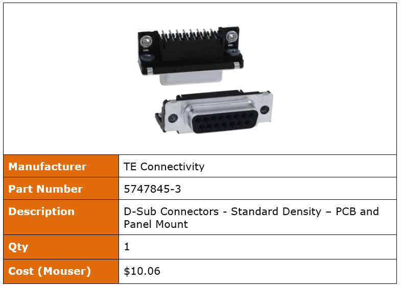
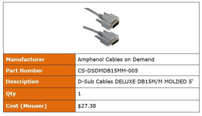
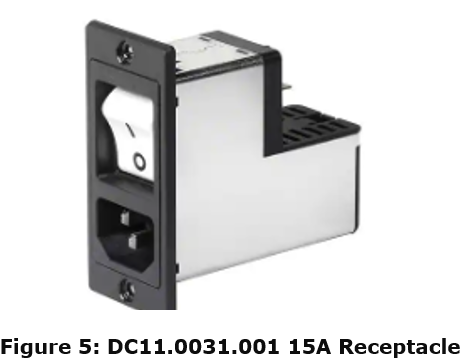
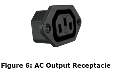
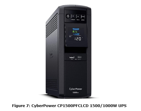
4. Power Interfaces: Power connectors must be rated for the high voltage 

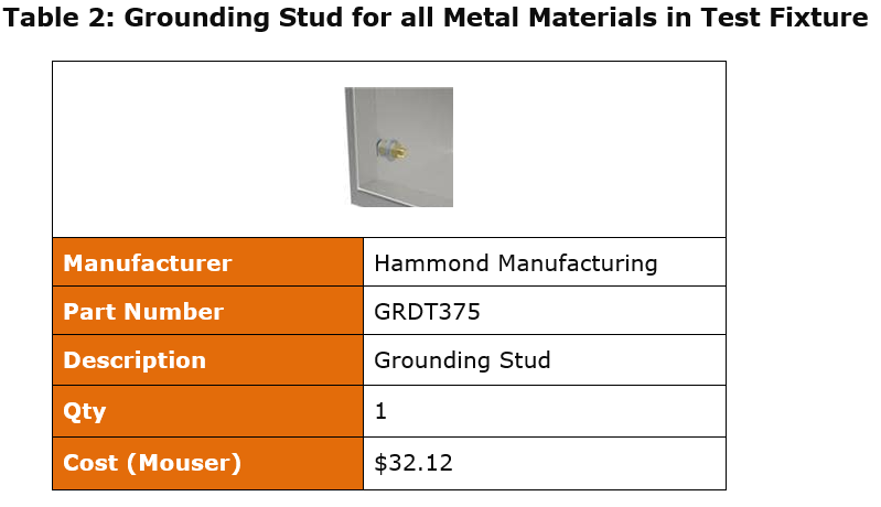
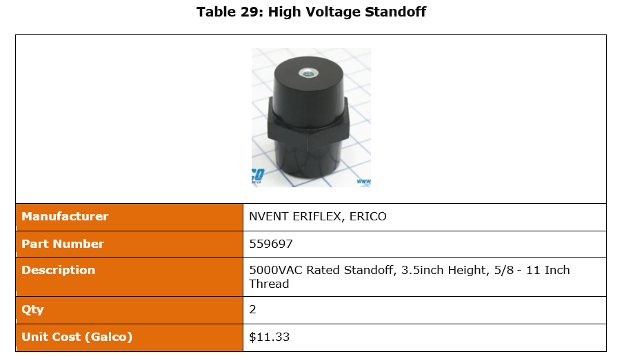
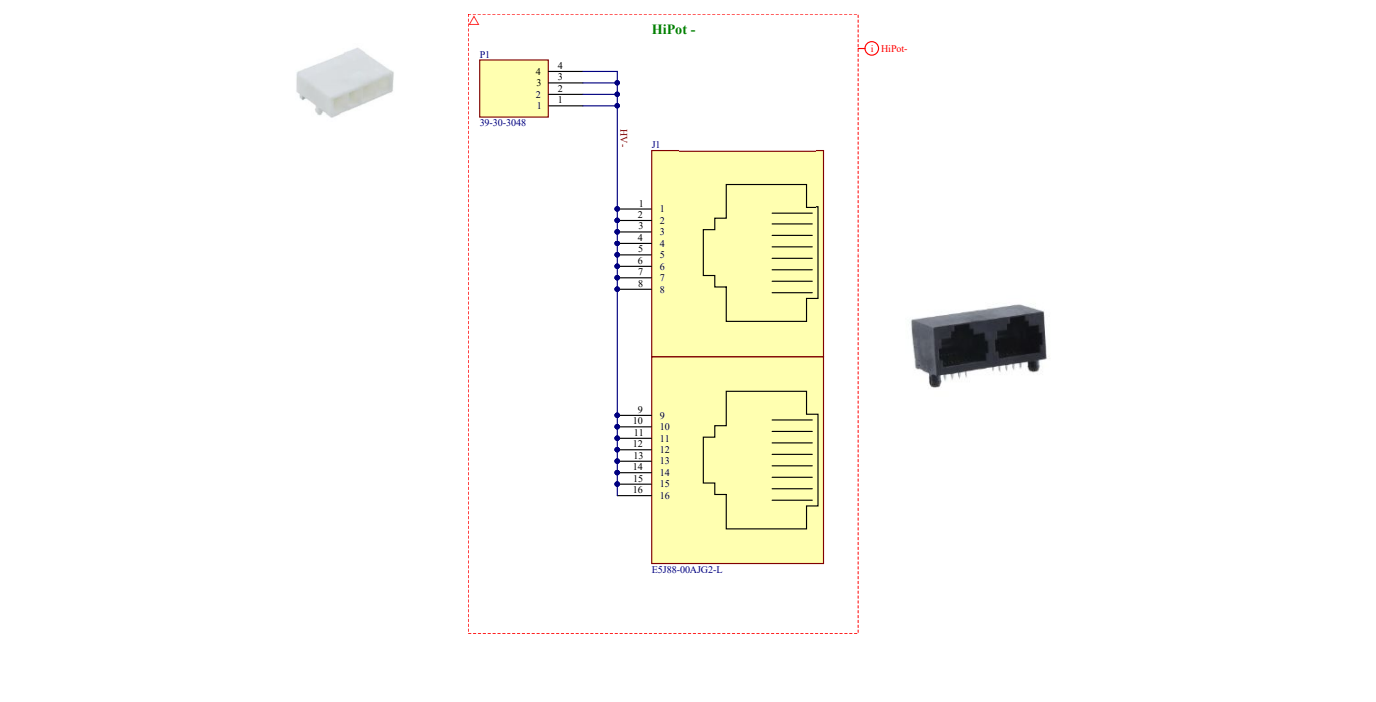
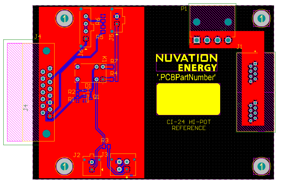
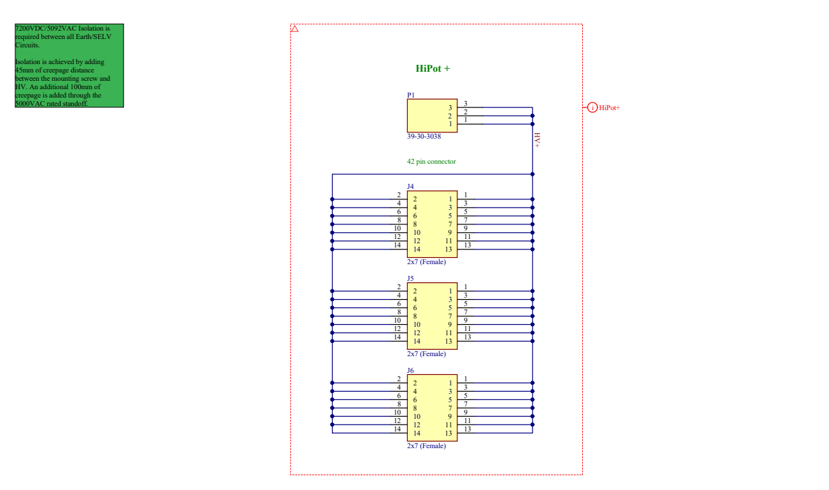
5. Creepage / Clearance: To meet CAN/CSA-C22.2 No. 62368-1-14 , and prevent voltage arcs, the design fixture including PCBs must be designed with this in mind. 

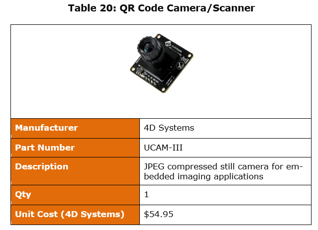
6. QR Code Identification: Every cell interface comes with a QR code. The test fixture should identify the QR code and log it in the database to indicate a pass or fail. 

7. Safety considerations:

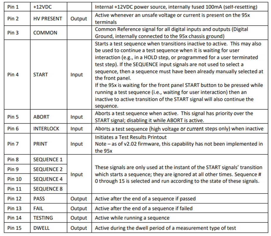
There are three conditions that must be met before the test PC can initiate the test:

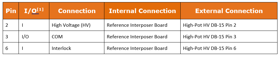
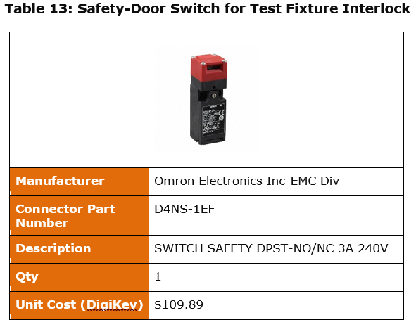
1. The test fixture is closed to eliminate any exposure of the internal connections. This allows for a safe energization of the Hi-Pot tester output. This condition will be detected by a proximity interlock switch.

2.The lid over the UUT is closed to ensure the user cannot access any high voltage pins, and to ensure the RJ45 connectors are connected to the CI. This will be detected by a second proximity interlock switch.

3. The QR code of the CI under test is read successfully. This ensures that there is a CI in the test fixture.

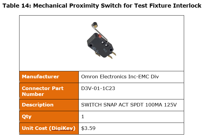
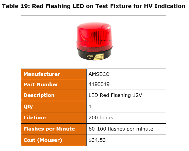
4. A third interlock switch will be positioned to detect when the UUT lid is open or closed and wired in series with the white LEDs. When the unit under test lid is open, the lights will turn off. This will reduce the number of hours the LEDs are on and therefore increases their lifetime.

Roles and Responsibilities 

1. Authored the Hardware Design Description and Manufacturing Test and Verification Plan documents 

2. This included designing the architectural block diagram of the test fixture, selecting every component, designing the PCBs, and developing the power budget

3. Defined the mechanical concept of z-axis jig, lid actuation, and interlock safety strategy. 

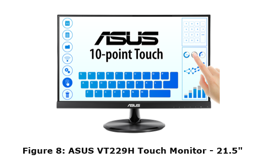
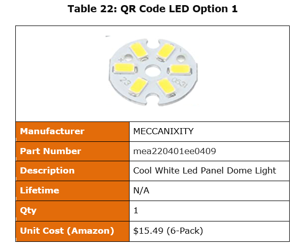
4. Specified that the QR code needs illumination for the camera to properly scan it

5. Determined creepage and clearances required everywhere to meet the specifications for safety

Technical Approach and Design

Step 1: Identify the main components such as Hi-Pot Tester and Test PC so I can determine how to create a block diagram around it

Vitrek 953i

Important Pins:

Pin 2: HV Present will be used to activate a flashing LED

Pin 3: COM needs to be connected to the PCB which handles interlocks and HV present.

Pin 6: When interlock is low, the system is inactive and won’t perform a test. 

HV+/- : Used to output the high test voltage

Power Input: Needs 120VAC and will be powered from the test fixture 

Test PC

The Test PC will connect to the Hi-Pot Tester with a RJ-45 Cable

Step 2: Develop the Block Diagram

  • HV Present will interact with a relay circuit to turn on a 12V flashing LED. Need 200mA of current so a AC/DC converter is needed
  • Interlock circuit is on PCB #1
  • LV- is connected to PCB #1 to isolate HV+ and HV- on different PCBs and to convert it to RJ45 connectors for the Cell interface
  • A daughter board is used because it will allow for:
  1. A flush, small opening to plug the cell interface in
  2. The connector between the cell interface and HV+ experiences the highest number of mating cycles. It will allow to swap out the board to increase the lifecycle of the test fixture without replacing the HV+ interposer PCB. 

For ex: Connector  has 1000 mating cycles. The HV+ board doesn’t need to be replaced until 1,000,000 cycles 

Step 3: Select Remaining Components 

All exposed metal is hard-bonded to a single grounding stud, so the chassis sits at ~0 V and provides a low-impedance fault path to earth if anything ever arcs/leaks.

All metal parts → grounding stud → AC inlet’s PE (green/yellow) → UPS → building earth.

Pin 2,3,6 Connect from Hi-Pot Tester to internal PCB #1 for the relay and interlock circuit. 

This receptacle includes a built in on/off switch which will allow for an additional layer of safety

To power the Hi-Pot through the UPS and line filter, a female receptacle is needed to be mounted on the test fixture.

To protect the Hi-Pot system against brownouts, fluctuations, and power outages a CyberPower CP1500PFCLCD 1500/1000W UPS is used. At full load (1000W) the UPS can run for 2.5 min and 10 min at half load. The UPS will connect to the Test PC via USB so that the PC can capture the status of the UPSs and go into a shutdown routine in case of power supply outage.

Qty:2 Same switch is used to turn on LED when Lid is closed. 

Creepage / Clearance Design

This will clarify the safety creepages and clearances associated with a voltage rating of up to 14.4kV (safety factor 2). A CI can support up to 1500V, however, the Hi-Pot tester will be set up to a voltage of 7.2kV to ensure the CI will function properly for a long duration.

For the PCB assembly to meet the electrical safety standard outlined in CAN/CSA-C22.2 No. 62368-1-14 for 14.4kV operation, material group IIIb, and pollution level 2, a creepage distance of 14.4cm is required between all electrically conductive material, components, and earth, through insulative material. 

This applies to the same components with 40.2mm of clearance separated by an air gap. 

To meet this:

1. Two Interposer PCBs will be used and spaced apart according to the creepage/clearance distances. 

2.The high-voltage interposer board will be mounted with high voltage standoffs to meet the creepage requirements.

Step 4: Schematic Design

PCB #1

With the diode:

  • When Q1 turns off, as soon as the node tries to rise above +12 V + V_F, the diode forward-biases and gives the current a closed loop:
  • The drain node is now clamped near +12 V + V_F. The MOSFET sees only a small rise, so no large spike, no avalanche, and much lower EMI.
  • The current decays because With the diode conducting, the inductor sees about −VF across it, so:
  • 12 DC PS for the Flashing LED and QR Light
  • 4 Pin Connector which allows for LED to plug in and is a completed circuit when interlock switch 3 is closed
  • Pin 2 HV Present is an active high of 5V.  It will cause VGS to be greater than Vth (1V)
  • The current will pass through the coil (960 ohms) which results in 12.5mA Ids. 
  • The contact will close and the LED will draw 200mA
  • Population option to add a schottky diode to protect the switch when the coil is deenergized.

With no diode: When mosfet turns off, Inductor current can’t change instantly (v=Ldi/dt), so the coil generates the voltage needed that pushes current the same way through the coil. 

  • With the channel open, the only way to keep that current is to shove charge somewhere. The coil flips polarity so that its MOSFET end goes positive relative to its +12 V end.

  • That forces the MOSFET drain node to rise above +12 V—sometimes tens of volts—until something conducts (stray capacitances or the MOSFET’s own avalanche at V_DS(BR)).

  • Current then decays fast because the coil now sees a large reverse voltage, but you get a big voltage spike/EMI, and the MOSFET must absorb the energy E = (1/2)L(Io)^2

PCB #2